New Disruptive Microchip Technology
GAA, Backside Power Delivery and the Secret Plan of Intel
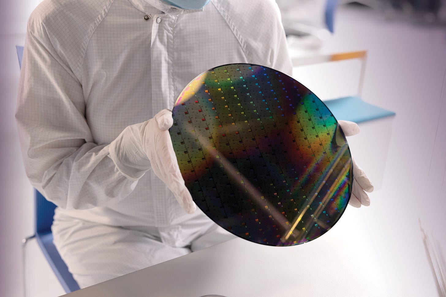
The world runs on silicon chips. Almost all of the world’s chip supply today—about 90% of it—comes from TSMC fabs. They started with 3-micron technology in 1987 and have now progressed to mass-producing chips at 3nm. Recently, they announced new technology that enables chips at 1.6nm.
These new transistors involve two interesting innovations: novel transistor architecture and backside power delivery. This has never happened before—a separation of the power interconnect from the signalling. As a chip designer, I can tell you that this is a big deal for the entire industry. To understand the complete picture, let’s start with transistors first.
Transistor Evolution
All modern computer chips are made up of transistors—tiny electrical switches that can be turned on and off. This is what a classical planar transistor looks like. It contains a gate, a source, and a drain arranged in a two-dimensional plane.
The device is controlled by the gate, and when we apply a certain voltage, or more specifically, a certain electric field to the gate, it opens the gate and current flows from the source to the drain.
As planar transistors have been scaled down, we’ve shrunk the size of the transistor, specifically the channel. Here we faced many problems, with excessive leakage being just one of them. Eventually, the solution was to completely change the transistor—from planar 2D transistors to three-dimensional FinFET transistors. Basically, they took a planar transistor and stretched the channel up as a vertical fin.
While in a planar transistor the conductive channel is only on the surface, with FinFET we have a conductive channel on three sides, while the gate is wrapped around it. Compared to the original planar transistor, FinFETs are more compact, so with FinFET we are now able to pack more transistors onto the same silicon die.
The first commercial FinFET devices were introduced by Intel in 2011, when I was still in university. A few years after Intel’s first FinFET device, Samsung and TSMC started fabricating 16nm and 14nm FinFET chips. Since then, TSMC has led the evolution of FinFET. Nowadays, all the cutting-edge chips are built with FinFET. For example, the latest AMD and Apple chips use 5nm or 3nm FinFET technology.
Gate-All-Around
However, FinFET technology has already reached its limit in terms of how much we can squeeze it in, how high fins can go, and how many fins can be placed side by side. Once again, high leakage has become a huge problem. Hence, to further shrink transistors and drive down costs, the whole industry is now moving to the new Gate-All-Around (GAA) transistor technology.
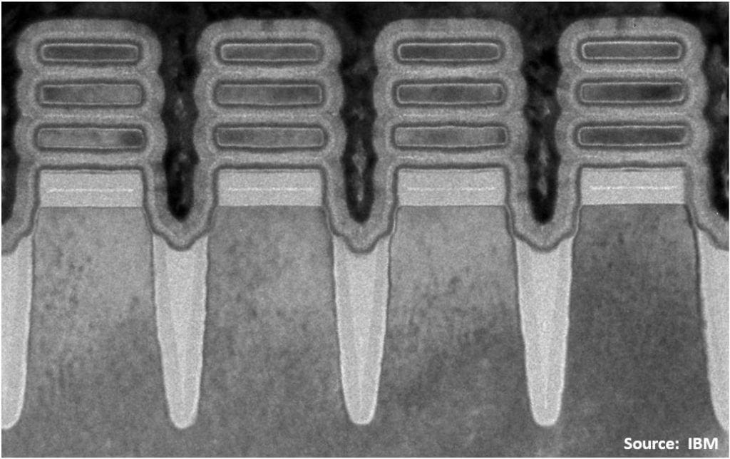
I’ve talked about it for years now, but it’s finally going into mass production. TSMC will shift to GAA technology for their N2 process node. They call it “nanosheet transistor”, but at its core, it’s essentially the same thing, just another term for the same concept. TSMC plans to begin production of chips based on GAA technology in early 2025, with the first ones expected to appear in iPhones.
Basically, they took the FinFET structure and turned it horizontally, placing several of these sheets on top of each other so that we can multiply the number of fins vertically. The best part is that the gate is completely wrapped around the channel, allowing us to better control it. With this innovation, we can slightly reduce operating voltage and significantly reduce leakage current. This will give us about 15% improvement in speed and transistor density, but the biggest gain with this technology is in power efficiency. GAA transistors consume up to 35% less power than FinFET technology, and this is huge. This is crucial for applications like mobile chips, where it could significantly prolong battery life, or for AI or HPC applications, which are usually very densely packed and power-hungry.
Backside Power Delivery
Earlier this month, TSMC debuted A16 technology on their roadmap, where 'A' stands for angstrom. TSMC’s A16 technology will be based on nanosheet transistors with one very interesting twist—backside power delivery. This innovation will be a game-changer in terms of power efficiency—let me explain.
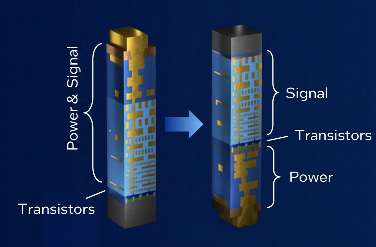
Ever since Robert Noyce made the first integrated circuit, everything has been located on the top, on the front side of the wafer, with all the signal interconnect and power delivery coming from the front side.
Backside power delivery is a huge change because we will move power lines underneath the substrate to free additional space for routing on the top. You know that when it comes to modern chips, there are billions of transistors that are interconnected with each other; so there are many levels of signal interconnect going over the chip. At the same time, there is a power mesh on top, which is a network of power and ground lines that distribute power across a semiconductor chip and provide the power supply to the transistors. Currently, all of the interconnect and power delivery come from the top, in different metal layers. Now imagine that when we move all the power to the backside, this will massively reduce the complexity of the wiring, letting us place and route transistors more densely and improve congestion.
This concept of separating power from signals will give more freedom to the routing Electronic Design Automation (EDA) tools. This change will not only affect the manufacturing flow but also the chip design itself. It will require a lot of learning throughout the flow, especially when it comes to the power mesh and heat dissipation.
TSMC will start producing chips based on A16 technology in 2026. I’m really looking forward to seeing how it goes. Of course, TSMC is not the only one working on this innovation. Intel is also trying to regain its position in the chip manufacturing race by working on backside power delivery as well as other upgrades.
Intel’s Moonshot
I want to spend some time discussing Intel’s ambitions because there are several interesting aspects to this story. For the past five years, Intel has lagged behind TSMC and Samsung in advanced chip manufacturing. But now, they plan to be the first, even ahead of TSMC, to bring new transistor and power-delivery technology into production.
For Intel, GAA technology and backside power delivery are coming together in the 20A process node. They are now putting the final touches on it. This 20A node is crucial for Intel. It's a risky move for Intel because typically, you want to introduce innovations one by one to understand where the problems are coming from. Introducing two new technologies at once means Intel is going “all in.” This is clearly a “moon shot” for Intel, with a lot of risk, because the probabilities multiply.
Interestingly, in the past, Intel used to be conservative while TSMC was more risky. This time, it’s the other way around. Intel needs to secure large buyers to reach a high volume and make the economics work because chip manufacturing relies on economy of scale.
In 2021, Intel CEO Pat Gelsinger promised investors and customers five nodes in four years. They have to deliver this time. They currently have Intel 4 and Intel 3 FinFET technologies in production and plan to mass-produce Intel 20A by the end of 2024. Arrow Lake will be the first Intel CPU to feature GAA (they call it RibbonFET) transistors and backside power delivery, which Intel calls PowerVia.
Intel 14A and New High-NA EUV
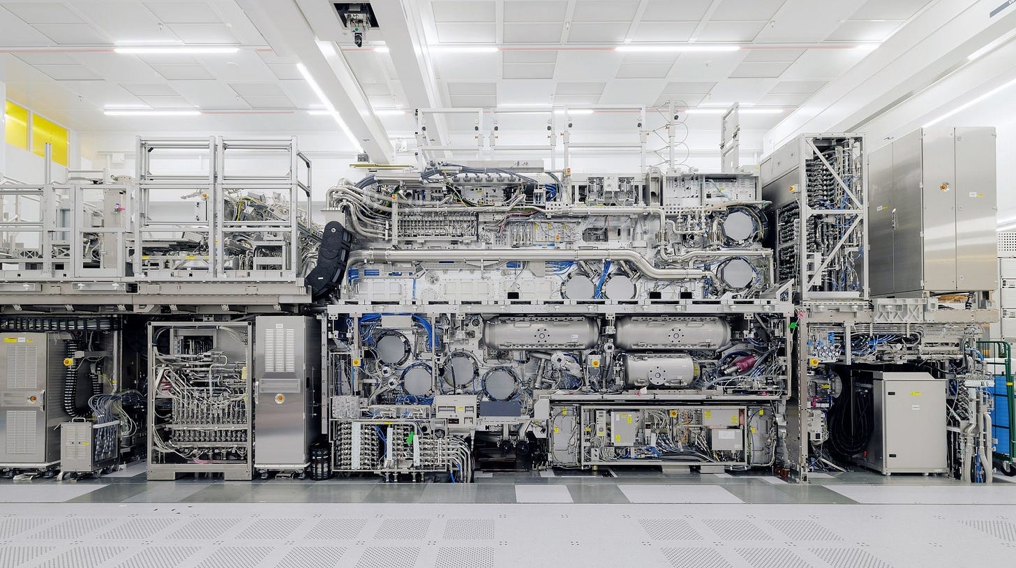
The most interesting milestone on Intel’s roadmap is the 14A process node, planned for 2027. This involves a significant update: using the new High-NA EUV lithography machines from ASML, each costing $380M. This comes with a lot of risk. Apart from the risks associated with new tooling, the economics of High-NA haven't worked so far.
In the competition between TSMC and Intel for sub-3nm nodes, it comes down to who can produce it first with good yield and at the minimum cost. High-NA EUV machines are not yet economically viable, with a high price per wafer. This is why TSMC is passing on this machine for now.
Direct Self-Assembly
At the moment, with High-NA EUV machines, the lithography process takes more time per wafer. This limits fab throughput and drives costs up. To make the economics work, Intel plans to use direct self-assembly. To put it simply, the wafers are covered with PMMA (poly methyl methacrylate) and baked. In this process, the polymer materials self-organize into tiny lines. Research suggests that EUV machines can help to guide this process on the wafer. However, this approach has been in the research phase for at least a decade due to high defect rates.
I’m rooting for Intel here, but given the innovations Intel is trying to pull together in the next few years, the risks are high. Let me know what you think in the comments. I hope Intel can make it happen because I love what they’ve done for the industry. If they manage to achieve a decent yield, especially with the 14A node, it will be a pivotal moment in Intel’s history, attracting some of the biggest customers and boosting their stock.
The advanced FinFET and GAA transistor architectures wouldn't be possible without ASM's equipment and process technology. Let me explain.
As we scale transistors down, we need to deposit ultra-thin layers, making precise techniques like Atomic Layer Deposition (ALD) essential. ALD allows the deposition of materials on the wafer atom by atom, creating layers just one atom thick. Leading fabs like TSMC and Intel use ALD machines from ASM for this purpose. ASM, a Dutch semiconductor equipment company, is a pioneer in ALD technology with a 55% global market share. Learn more about ASM and their products here. Thank you, ASM, for sponsoring this edition of Deep In Tech Newsletter.


Fabulous summary of the exciting race to bring better technology to the world. It will be good for all of us if Intel’s high risk approach of bringing two advancements simultaneously works. Often: “who dares wins” & so we can hope with good reason. Thank you for sharing!
From the opening paragraph: " Almost all of the world’s chip supply today—about 90% of it—comes from TSMC fabs."
Did you mean to say almost all of the worlds chip supply with a particular geometry such as 3 nanometer are from TSMC, or that most of the chips with backside power delivery come from TSMC?