New Memory Technology
and the end of SRAM scaling
Let me just tell you straight: SRAM memory scaling is dead. It's a fact, and it will affect the entire industry. This is a huge problem for NVIDIA, Intel, Apple, AMD, and pretty much every chipmaker and startup. Now for the good news: there is a new memory technology that may solve this problem. It can actually bring computers one step closer to a major boost in speed and reduction in cost. Let me explain.
We need more memory
Ever since transistors were first invented in 1947, we have always found ways to shrink them down year after year. We did a great job with this: the first transistors were in the range of centimetres, then micrometers. Now we’ve progressed to mass-producing chips at 3 and 4 nm. For example, Qualcomm’s Snapdragon X Elite chip is in N4 process node, and the latest Apple M4 chip is in N3. For a long time, memory also followed this beautiful trend, scaling along with circuit logic. But it’s now over, and that’s a huge problem for the entire industry.
Over the past 60 years, SRAM has been the memory of choice in all applications where speed and fast access time are needed. SRAM consists of latches, usually built with four to six transistors. We love SRAM memory because it tends to perform better and drain less power, especially when it is idle. It’s the highest-performing memory there is, and it’s integrated directly alongside the logic of the cores. It stores data close to the cores, and since we still use GHz rate clocks, we can access it in the 250-500 picoseconds range.
The general trend is that the amount of memory per chip is constantly increasing. If we look at all of the recent chips developed by Intel, AMD, NVIDIA, and Apple, etc., all of them are adding more and more memory to their chips. For example, NVIDIA is packing more and more cache into each of their new GPUs. Similarly, Apple is dedicating more and more area to larger caches with each new generation of its M chip. The problem is that cache memory doesn’t scale as well as logic, and as a result, it’s eating up a larger and larger part of the chip.
Scaling problem
Let’s try to understand what’s going wrong here. In comparison to all other types of memory, SRAM is a part of the chip die itself and it’s fabricated in the same process node as the chip logic. The chip logic has more or less followed Moore’s law, giving us approximately 2 times the transistor density with each process node for the same price. Unfortunately, memory cells don’t scale at the same rate. At first, memory scaled as a factor of 1.8, then 1.4, and with each process node this number has gotten lower and lower.
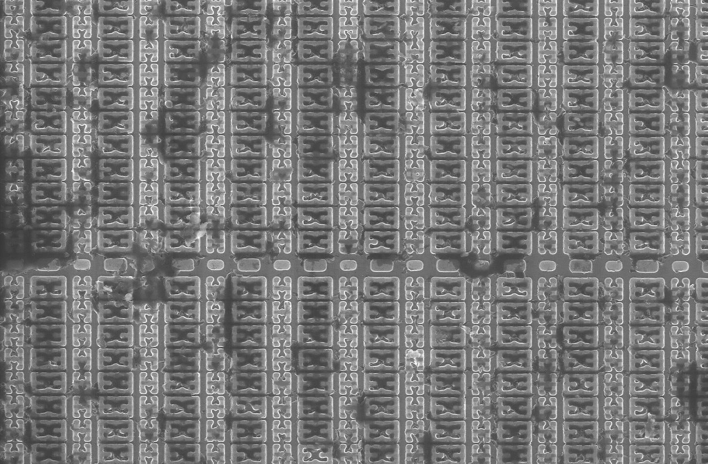
At the point when TSMC announced their latest N3 technology, it had become clear that SRAM scaling was dead. The N3 node actually delivered a factor of x1.7 transistor scaling and x1.0 scaling of SRAM. As you can see from the chart above, bit cell size has an area of 0.021 µm², which is exactly the same size as at their N5 node, and with the next improved N3B process node it’s scaled by just a measly 5%. It's not just a problem for TSMC; the same issue is affecting the entire industry including Intel and Samsung fabs.
Why doesn't scaling work? Simply put, these memory cells are special. Despite being constructed from transistors, the SRAM cell itself has a unique structure. It's a highly sensitive device that is very vulnerable to manufacturing process variations such as transistor threshold voltage or dopant fluctuations. It appears that any variations in the fabrication process prevent further scaling of smaller memory cells. The situation may not improve and could worsen as we transition from FinFET to GAA technology, replacing fins with nanosheets, which introduces new technical challenges.
Thus, it's increasingly inevitable that with each new process node, SRAM consumes more chip area, driving up costs. The major issue here is that we can't do it without SRAM. If a processor core lacks sufficient SRAM, data must be retrieved from further away, requiring more power and resulting in slower performance.
Chiplets
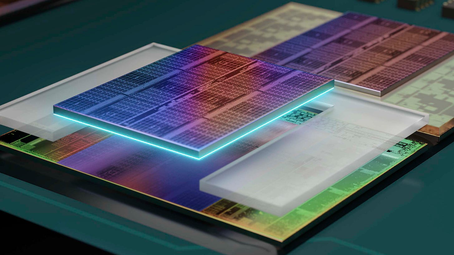
So when we realised that we couldn’t scale SRAM any further, we found another option - chiplets. Simply putting memory right on top of the cores. It was a huge deal when back in 2022 AMD first introduced their V-cache technology and this was huge because with that we can get a lot more of cache memory. Here we must give a lot of credit to AMD for their progressive thinking. Of course, as always a part of the credit should go to TSMC, because AMD used TSCM’s 3D SoIC "System on Integrated Chips" (SoIC) packaging technology. They basically stacked an additional 64MB of L3 cache directly on top of the CPU die and this additional cache gave a huge performance boost to many applications, including gaming.
In general, this idea of stacking things vertically on top of each other is brilliant. One of its biggest advantages is that you can mix and match chiplets in different process nodes. For example, you can build a chip using the most advanced process node for the logic and then on top stack any memory die, for example in one of the older process nodes. In this case we can benefit from the improved speed and density in the core’s logic and then use a bigger SRAM on top, or we can also use an older SRAM die which is cheaper, more reliable and has better yield.
New Memory Technology
Chiplets may help to reduce costs and maybe increase memory, but it’s not really solving the problem. That’s why for a long time now the industry has been looking for an alternative memory technology. So there are several emerging memory technologies, including Magnetic RAM, Ferroelectric RAM, Resistive RAM, Phase-Change Memory, and others. What’s interesting is that each of these types of memory technology have their pros and cons - some of them are more optimised for area, some for power or speed, some have faster access times and higher bandwidth than others. On top of that, we know that each CPU or GPU has several types of memory, each of them have different requirements. The main differences are in their data storage mechanism and their speed.
SRAM is the fastest, with access times in the range of nanoseconds. and it has to be low power. DRAM is slower, and is based on just one transistor and a capacitor, and here the access time is in the range of tens of nanoseconds. Flash memory is the slowest. And then we have to distinguish between volatile and non-volatile types of memory. SRAM and DRAM are volatile, so they retain data only as long as power is being supplied
So now it’s clear that when it comes to SRAM memory, the most critical things are latency, area and power consumption. So in the new paper published in Nature researchers at Stanford have developed a new PCM material called GST467 that uses chalcogenide alloy in a superlattice structure. It’s basically a memory cell consisting of a glass material sandwiched between two electrodes, and when we apply a high current pulse to it, it switches between the crystalline and amorphous states. I explain it in more details in this video.
And this new technology has really high potential because it checks all of our boxes. It has fast access time in the range of nanoseconds. It works at a low operating voltage, so it’s compatible with modern logic processors. According to the paper, it has the smallest dimensions to date (0.016 um^2) and it's actually denser than, for example, TSMC's SRAM in the 3N process node. From the standpoint of area, it's about 23% more efficient. That’s amazing!
Of course, it’s brand-new research, and there are many technical challenges remaining until it can achieve widespread commercial adoption. One of the challenges is integrating it into the existing CMOS manufacturing flow, reducing the programming current, improving reliability, etc.
Outlook
Clearly, there is an ongoing trend where we pack more and more memory into chips, which is becoming even more critical with the rise of AI-based applications. I believe that the SRAM technology as we currently know it, based on latches, won’t go anywhere for L1 and L2 cache, at least for the next couple of decades. So, we’re going to see it consume more and more area and money. Afterward, we will see new memory technologies first coming to DRAM and potentially to L3 cache as soon as they can achieve fast enough access times, within the range of a few nanoseconds.
I think the current "dead end" situation with SRAM will compel us to work on further innovations, and it's going to be exciting to follow.
Let me know your thoughts in the comments. If you enjoy this post, please share it with your friends and colleagues.


A brilliant mind and exceptional hot! Keep us up to date. To have you close to us keeps us assured that pretty women (actually gorgeous ladies such as yourself) _can_ truly entertain a topic deeply connected to their minds ...into another's.... ! You'd be wonderous to lay beside and listen to your inner thoughts on a topic of tech...arousing the very idea that you really enjoy many aspects of life all bundled together. -Hot. You're very hot Ana....
I enjoyed the article. I love following the progress of the technology you report on. My Father who started working with computer in 1953 or 4 always said as the companies and later his own personal computers were updated and replaced: "We are now working with the latest obsolete technology." I often look up reference to terms you use as I read. Today it was "chalcogenide alloy".