

New Semiconductor Breakthrough
It could sparkle a new era in electronics

Researchers from Georgia Tech, in collaboration with Tianjin University in China, have developed a new type of semiconductor material. With this new technology we will be able to build computer chips that will run orders of magnitude faster. This could really spark a new era in electronics. As a chip designer, I’m very excited about this work. Let me explain.
Beyond Silicon
According to Moore's Law the number of transistors in a chip doubles approximately every two years. This observation was first described by Gordon Moore in 1965. However, later Moore himself predicted that this rate would slow down. That’s unfortunately true. It is getting harder and more expensive to pack even more transistors onto a silicon die. It seems like we are hitting physical limits such as a size of an atom.

Still, there are lots of efforts made by companies like TSMC, IBM, Imec and Intel to continue shrinking transistors even further, and keep Moore’s Law going indefinitely. Right now, we’re in the ball park of 200 million transistors per millimetre square. That’s an impressive number! However, further scaling of transistors appears to be a huge challenge. One of the bottlenecks is the lithography process. To be more specific, we need more advanced lithography machines with shorter wavelengths of light, such as extreme ultraviolet, to be able to further shrink the space between transistors.

To move the needle forward, we are starting to build in the third dimension: stacking transistors on top of each other to fit more in the same area. Unfortunately, here again, we see a new problem emerging. Vertically stacked devices suffer from a heat dissipation problem. There is no heat dissipation path, which leads to overheating. IBM is trying to address this problem, and last year they introduced Vertical Transistors (VTFET), where the gate is placed vertically. However, these devices are still in the research phase.
Of course, researchers are constantly looking for new and novel semiconductor materials, which can offer even better speed and heat dissipation than silicon, and eventually replace it.
Graphene
For a long time, the researchers were investigating graphene as a possibility. In fact, gaphene is really appealing because of its particular crystal structure and its exceptional ability to dissipate heat. It has much higher thermal conductivity than silicon. Nowadays, heat is one of the major bottlenecks for many electronic devices. It degrades performance, seriously degrades lifespan or even can cause a meltdown. This new graphene-based semiconductor is much better at thermal management.
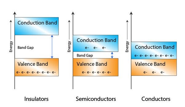
However, there is a fundamental problem with graphene. It’s actually not a semiconductor. It has zero-band-gap. This reminds me of when I was a student and had classes on semiconductor physics. Let me explain why band gap in semiconductors is a really big deal.
You know that all microchips are made up of transistors. Transistors are essentially tiny switches which can be turned on and off, and their states are controlled by voltages applied to the control terminal. The band gap in transistors is fundamental because it determines a minimum energy required to make a transistor switch between those states. Ideally we would like to have a material with a band gap that is small enough to allow some conductivity, but not too high, or else it’s an insulator. In contrast, when the band gap is too small, like in the case of graphene where it’s 0 eV, it becomes highly conductive, similar to metals. You see, zero band gap of graphene is a fundamental problem because we can’t make a graphene transistor function as a switch.
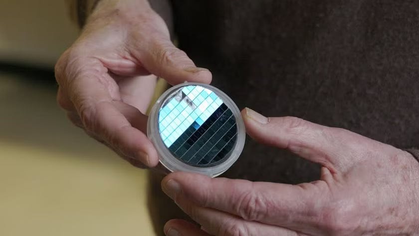
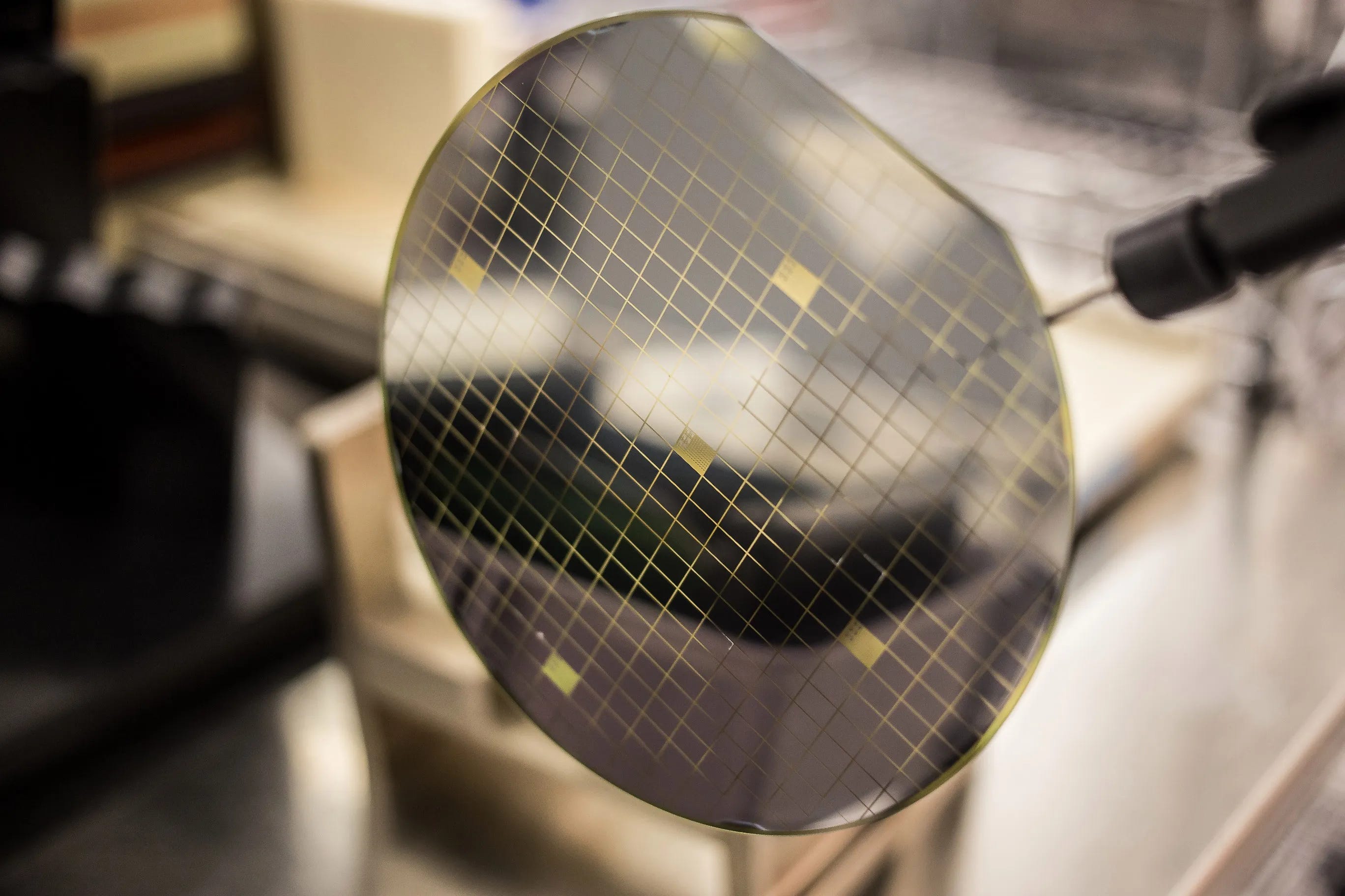
However, in this new work the researchers found a way to make a perfect semiconductor out of graphene. They grew graphene on top of Silicon carbide wafers. That’s pretty SiC 🙂 In the fab they heated up silicon carbide to very high temperatures, over 1000C and doped it. Doping a semiconductor has nothing to do with banned substances. It means electrical properties of a material usually by adding impurities. By altering the very properties of graphene, they’ve managed to introduce a bang gap. They called this new semiconductor semiconducting epigraphene or SEG. If you want to know how a graphene transistor works, check out this video.
What’s amazing is that these new transistors are capable of switching very quickly. It means they can now support very high terahertz-range frequencies. This is possible thanks to the high electron mobility of graphene. In this work, they were able to achieve electron mobility 10 times higher than what’s currently possible with silicon chips. In practice, this means an electron can move much faster through a semiconductor, which promises much faster chips with less heat dissipation.
I think, If we can figure out the graphene based chips, it will be huge. There are still many technical challenges to overcome to bring this epigraphene technology to mass production. I think it has a good chance of playing a pivotal role in the future of semiconductor technology. As always, let me know what you think in the comments!
What do you know about the new advancements in memcapacitors or chips which use electric fields instead of electric current to calculate? Curious on your thoughts?
With SiC becoming more dominate in the “power” segment and in chiplet stacks do you think this new advance will allow Chinese companies to compete & maybe even surpass current state of the art advanced chips <7nm even while being at lower density?