NVIDIA reported a record high revenue of $30 billion for the quarter, and their datacenter revenue more than doubled over the past year. Despite this impressive job from NVIDIA and earnings that beat estimates, NVIDIA's shares plunged. What’s going on here?
Apparently, one of the reasons has to do with concerns over NVIDIA’s next-generation Blackwell GPUs being delayed. Many reports are indicating that there are several flaws with the new packaging technology of Blackwell GPUs… and I’ve dug into this.
The general trend in the industry is that we are shifting towards larger GPUs because AI models are growing exponentially in size and the amount of data processed by AI models is also increasing. Larger chips can handle more data simultaneously, improving the speed of training and inference. Following this trend, in their new Blackwell GPU NVIDIA introduced a double-die design.
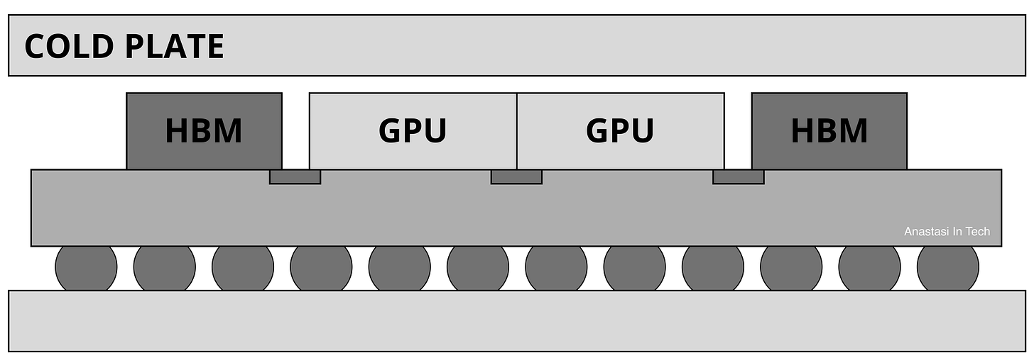
The Blackwell GPU features two large GPU dies that contain the core logic and are linked by a very fast, 10 terabyte per second interconnect bridge. Through this bridge, one die communicates with the other, and every die is surrounded by 4 memories. To package something as complex as this, they use CoWoS-L (Chip on Wafer on Substrate, L stands for "Local Silicon Interconnect") packaging technology from TSMC.
If we look at the cross section of NVIDIA Blackwell GPU, here we have a substrate and an organic interposer soldered on top of it. The memory and logic dies sit on top of this interposer and are interconnected through tiny bridges so called Local Silicon Interconnect (LSI).
Challenge #1
Blackwell GPU is actually an iteration of their previous generation, the Hopper GPU, which had a single GPU die talking to six memory dies and the package was almost half the size of the Blackwell package. The Blackwell GPU is a much larger chip, so they decided to go for CoWoS-L TSMC's Chip-on-Wafer-on-Substrate packing which allowing a bigger packaging design with up to 12 memory dies and at lower costs compared to CoWoS -S packaging.
Now manufacturing this new Blackwell GPU is getting very challenging: by assembling all 10 pieces together on top of the the interposer, it has to be very precisely aligned with the pins on both the memory and logic die sides. There are many thousands of connections in between, so aligning them is not easy. However, the trickiest part is actually aligning these two logic dies to enable 10 terabyte per second communication
Challenge #2
That’s the first challenge, and NVIDIA is working with TSMC to optimize the process, and is assembling and scaling it up to manufacturing at high volumes. However there is a second challenge - thermals, or thermal management. This topic is addressed in several scientific publications and is indeed a challenge.
This problem arises from the fact that the coefficients of thermal expansion of various materials differ. In this case, we have memory, logic dies, an interposer, and a substrate—each with its own thermal coefficient. When the GPU is operating, it heats up. These temperature changes cause structural deformations, generating stress in various directions. An additional issue is that different materials expand at different rates, making the entire process dynamic, which can lead to stress gradients, relative die shifts, and connection failures between dies.
No doubt, NVIDIA has already tested this approach on prototype chips, but apparently, the issue is more complex. In my opinion, the dynamics under real application loads play a significant role here, and this aspect is very hard to simulate and predict. Let me know what you think in the comments.
Below I discuss the steps NVIDIA is taking to address this issue and provide my outlook on the situation.
Keep reading with a 7-day free trial
Subscribe to Deep in Tech Newsletter to keep reading this post and get 7 days of free access to the full post archives.


