
So today let’s have a look at the two hottest headlines of the last weeks: NVIDIA’s Blackwell GPU and the new 4 trillion transistor AI Accelerator from Cerebras.
Nvidia
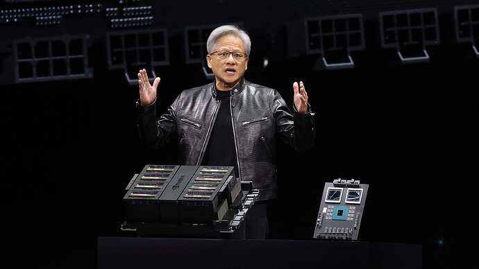
Nvidia’s now at the top of the world. We’ve never seen such profitability from a hardware company. That’s just one of the reasons my investment portfolio has been performing great 😊. Now they’ve revealed the new Blackwell GPU. This GPU is providing four times the training performance, and up to 30 times the inference performance, compared to the previous generation, the Hopper H100 GPU.
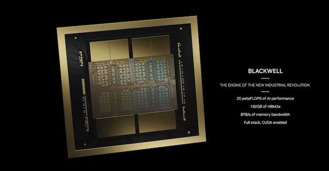
First of all, let’s discuss how they managed to achieve this fourfold performance improvement. Part of this is enabled by a dual-chip design. The Blackwell GPU is built out of two silicon dies in a single package that are linked by a very fast, 10 terabyte per second, connection. Therefore, we can consider it as nearly a single GPU with 208 billion transistors and 192GB of external memory. This GPU is capable of 20 PetaFLOPS of AI performance. Fantastic, right? Absolutely. But make sure to keep reading to understand how to come to ZetaFLOPS performance.
As a first step, to double its performance, NVIDIA had to double the area. It was an expensive decision because the price per chip is actually price per area, which depends on the technology node and the volume. In fact, NVIDIA had to keep using the N4P process by TSMC, which is the same node as it is for the Hopper GPU. This is a refined version of the N4 with a 6% transistor density boost and 22% more energy efficiency over the N4. NVIDIA had to continue using N4 process node due to TSMCs struggles with N3 technology. This situation impacts not only NVIDIA's roadmap but also those of AMD, Intel, and other chipmakers.
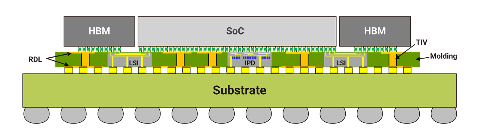
In a bid to maintain its competitive edge, NVIDIA has introduced a double-die design packaged using CoWoS-L packaging technology from TSMC. CoWoS-L technology is used to integrate multiple dies side-by-side to achieve better interconnect density. Now if you consider the dual-die design and the packaging, the costs of fabricating this GPU is more than double compared to Hopper GPUs. So they definitely will not be able to achieve their legendary 85% margins as they previously did. They had to make a trade-off here to remain the frontrunner in AI GPU performance, as the competition is heating up. All the hyperscalers Google, META and Amazon are now developing their own custom silicon. AMD and Intel also want a piece of this pie. Startups like Cerebras and Groq also offer some excellent alternatives. NVIDIA is definitely the leader in AI hardware and they are making great efforts to stay so, but the competition will not let them rest for a moment. Please let me know what you think in the comments!
Precision
We have seen so far that doubling the silicon can double the performance, but where does the second double fold come from? It clearly doesn’t come from a smaller transistor technology, but from using a new numbering format and in this way it lowers the precision of the calculations. For most computations within a neural network, computing every digit, say the 20th, is unnecessary; the network can achieve the same task with similar accuracy at a lower precision level. That’s precisely the trick here. By reducing the precision of calculations, for instance, employing a 4-bit format instead of 8-bits, we can conserve half of the on-chip memory. Smaller numbers facilitate faster computation, consume less energy, require less memory bandwidth, and demand less silicon for mathematical operations.
It all started with their previous Hopper GPU, in which they introduced a transformer engine which can dynamically change the precision of the calculations, so that transformer neural networks can be trained faster. In the previous Hopper GPU, they used floating point number formats with 8-bit precision. But with Blackwell, they’ve taken this one step further. In the new architecture, the units do matrix multiplication with numbers just 4 bits wide. This is another area where an improvement in performance comes from. I think it’s pretty low and that makes me curious me to see how well is gonna work for inference applications. Now I’m looking forward to seeing real world benchmarks.
Cerebras
Now, let's discuss the new stunning 4 trillion transistor chip that was just announced by Cerebras. This one is pretty unique, and you can see that they are crushing Moore’s Law. You know, since the advent of microchips in 1972, the semiconductor industry has followed Moore’s Law, which states that the number of transistors on a chip is able to double roughly every two years. As you can see from this plot, Cerebras seems to be outpacing this law, which many had believed was no longer applicable.

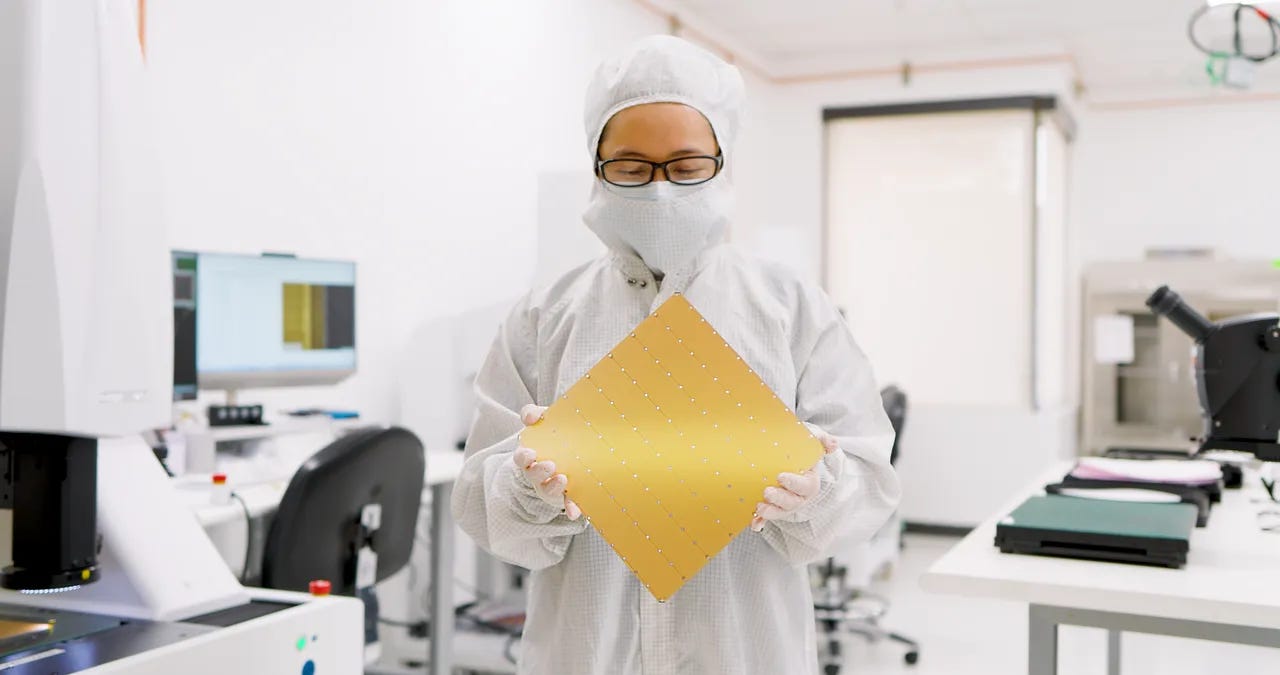
Their previous chip was fabricated at 7nm and the new one by TSMC, Wafer Scale Engine - 3, is at 5nm. The number of transistors on this chip has more than doubled since the previous generation thanks to a technology node upgrade. As we know, a huge part of this success is the success of TSMC, which can fabricate the wafers at 5nm at a very high yield.
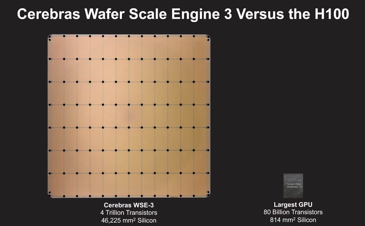
One of the main reasons why Cerebras has been successful is that they’re doing something different from everyone else. While a silicon wafer typically accommodates many chips (this is how it has always been done by companies like AMD, Intel and NVIDIA), they slice a 300mm wafer into, let’s say 65 GPUs. However, Cerebras takes the 300mm wafer and makes a single giant chip out of it. To give you a feeling of the scale of this, here is their Wafer Scale Engine 3 chip next to the H100 GPU. It’s 56 times larger than NVIDIA’s H100 GPU.
Going for larger silicon is such a great idea - it totally makes sense for today’s AI workloads and this seems to be a general trend in the industry.
"Hopper is fantastic, but we need bigger GPUs," Huang said during his GTC keynote.
Cerebras was doing it long before then. It’s beneficial because thousands of GPUs have to be used for a single AI task to be performed and interconnecting them, distributing the load efficiently is a complex and expensive task to carry out. By having one giant chip, you can significantly reduce the costs and complexity required.
WSE-3 chip features nearly 900,000 AI cores and 44GB of memory. When it comes to memory, in this case it is on-chip memory that is intertwined between the computing cores, that has the exact the same goal, to keep the data and compute as close to each other as possible. This is another architectural difference compared to NVIDIA and AMD GPUs which utilize off-chip memory

This new AI chip is designed to train the next generation of giant language models, up to 24-trillion parameters in size. Just imagine, this is 10 times larger than OpenAI’s GPT-4 and Google’s Gemini. Now they plan on connecting 2048 of them together to build an AI supercomputer capable of reaching up to a quarter of a zettaflop (10^21). Such a machine could, for example, train an LLM Llama 70B model from scratch in just one day.
To give you a sense of how high the demand is for AI infrastructure, here is a recent quote from TSMC’s founder, Morris Chang:
“We’re not talking about tens of thousands of wafers. We need so many fabs. We need three fabs, five fabs, 10 fabs”.
If you want to learn more, check out this video:
Let me know what you think and let’s connect on LinkedIn.